

Today, I'm going to give you a thorough overview of Diode. In this blog, we will start with the basics of a diode and cover all the points. We will discuss Diode working, symbols, Applications, Biasing conditions and so on.
Starting with a small description, A diode is a type of electronic component that permits the current to flow in just one direction. It has minimal resistance in one direction but extremely high resistance in the other.
Diode

From the word DIODE, "Di" means "two," and "Ode" means "electrodes," referring to a device or component with two electrodes, namely an an anode "+" (Positive) and a cathode "-" (Negative). A diode is a two-terminal electronic component that enables just one direction of current flow.
The diode is constructed from a mixture of two semiconductor materials, P and N. The positive side of the semiconductor is known as the anode, while the negative side is known as the cathode. Silicon is chosen in the fabrication of diodes due to high-temperature bears, although germanium is also used when a lower voltage loss is required.
SYMBOL
A diode's symbol is displayed below. In the forward biased situation, the arrowhead points in the direction of the current flow. As shown in the diagram anode is at the P side(left side), while the cathode is at the N side(right side).

CONSTRUCTION OF DIODE
Conductors, insulators, and semiconductors are the three types of solid materials that may be found. Semi-conductors can be either conductors or insulators depending on the potential applied to them. Conductors have a maximum number of free electrons, insulators have a minimum number of free electrons (negligible to the point where current flow is impossible). Silicon and Germanium are the most often used semi-conductors. Silicon is selected since it is abundant on the planet and has a wider temperature range.
There are two types of semiconductor material; Intrinsic and Extrinsic semiconductor
Intrinsic Semiconductors:
These are also known as pure semiconductors because they have an equal number of charge carriers (electrons and holes) at ambient temperature. As a result, both holes and electrons participate equally in current conduction. Pure semiconductors are the most natural.
Extrinsic Semiconductors:
Extrinsic semiconductors are used to increase the number of holes or electrons in a material by adding impurities (other than silicon and germanium or simply trivalent or pentavalent elements). Doping is the process of introducing impurities into pure semi-conductors.
Formation of P-type and N-type semiconductors
There are two layers in a semiconductor diode. A P-type semiconductor layer is on one side, while an N-type semiconductor layer is on the other. An N-type semiconductor and a P-type semiconductor are combined in a PN junction diode, with a terminal linked to each of the P-type and N-type semiconductor materials. P-type material is linked to an anode terminal, whereas N-type material is connected to a cathode terminal.
When trivalent impurities are added to silicon or germanium, the number of holes increases, resulting in a positive charge. As a result, this layer is referred to as the P-type layer.
When pentavalent impurities are added to silicon or germanium, the number of electrons present increases. As a result, this layer is referred to as the N-type layer.

The majority carriers in a P-type semiconductor are holes, whereas the minority carriers are electrons. An N-type semiconductor, on the other hand, contains electrons as the majority carrier and holes as the minority carrier.

Biasing Conditions
There are three possible biasing conditions for the PN Junction:
Equilibrium (zero bias)
In a PN junction, without an externally applied voltage, an equilibrium condition is reached.

Forward Bias
The migration of electrons and holes across the PN junction causes current to flow in forward biased situations. Connecting the positive terminal of the battery to the anode of a diode, and the negative terminal to the cathode. The voltage source linked to the diode(external supply) should have a value that is greater than the potential barrier. Because like charges repel one other, the negative terminals exert force on the electrons in the N region, causing them to migrate towards the PN junction.
The mobility of electrons causes current to flow through. We may deduce from this that current flows under forwarding biasing situations owing to the passage of electrons and holes.

Reverse Biased Diode
Let's examine what occurs when we connect the voltage source's negative terminal to the p-type side of the diode and the positive terminal to the n-type side. The holes in the p-type area would be moved further away from the junction due to electrostatic pull from the source's negative potential, leaving more exposed negative ions near the junction.

Similarly, free electrons in the n-type area would be moved away from the junction and towards the voltage source's positive terminal, leaving more exposed positive ions in the junction.
In a p-type semiconductor, there are always some free electrons, and in an n-type semiconductor, there are always some holes. Minority charge carriers are the charge carriers in a semiconductor that are opposing each other.
The holes on the n-type side would readily traverse the reverse-biased depletion zone in the reverse-biased situation.
As a result, a little current flows from the positive to the negative side of the diode. Because the number of minority charge carriers in the diode is so small, the amplitude of this current is quite minimal. Reverse saturation current is the name for this type of current.
Types of Diodes
A light-emitting diode is referred to as an LED diode. When current is passed via a diode LED, photons are emitted due to which it glows.
LEDs are fairly popular these days and may be found in almost any electronic device. The cost has been reduced to the point that they are now employed in circuits to signify board-level functionality.
Zener Diode
In the breakdown area, zeners have a much sharper current curve than normal diodes. These diodes can work in forward as well as in reverse bias mode. eg 1N4742A
Avalanche Diode
Avalanche diodes are those that are specifically designed to handle the breakdown voltage mode. As a result, they are not harmed when placed in breakdown mode since their design equally distributes the current density.
Typically, these diodes are employed to defend against undesirable or unexpected voltages. They can be set into breakdown mode, which allows them to transfer excess energy to the ground and save a circuit that was not meant to tolerate high voltages.
Germanium Diode
These diodes have a typical forward voltage of 0.3 Volts due to their material qualities.
This type of diode is useful in audio and FM circuits because of its lower voltage. Prior to the widespread use of Silicon diodes, this was the most common diode.
Gunn Diode
It differs from other diodes in that it is made entirely of N-type material (there is no P-type material in it). It consists of two N-type material sections joined by a thin N-type material segment. As the voltage across the device rises, the current rises until it reaches a point where it starts to fall.
They're often utilized in microwave electrons oscillator circuits, such as radar speed guns and automated door openers.
Photo Diode
When photons are absorbed by a photo diode, electricity is generated. As a result, these devices are useful for detecting photons at a variety of wavelengths.
In reality, every digital camera technology is based on an array of photo diodes, each of which is referred to as a pixel.
PIN Diode
PIN diodes are created by placing two undoped materials between two P-type and N-type materials.
In high-frequency circuits, these diodes prove helpful. They produce excellent attenuators and switches for RF and microwave signals.
A Schottky diode is one in which the P-type material is removed and the N-type material is combined with a metal to form the diode.
The benefit is that the forward voltage is reduced, which allows for higher switching frequencies in some applications. This, along with the fact that they recover faster, makes them helpful in circuits such as switching power supply.
Tunnel Diode
Tunnel diodes make use of a phenomenon known as quantum tunnelling.
The interesting thing about these devices is that current travels easily from anode to cathode at first. The current flowing through the device reduces as the forward voltage rises, resulting in negative resistance.
Then, when the voltage drops even lower, it begins to behave like a typical diode. They're helpful in circuits like frequency converters and detectors.
Following are the applications and uses of the diode:
- Diodes as a rectifier
- Diodes in the clipping circuit
- Diodes in clamping circuits
- Diodes in logical gates
- Diodes in reverse current protection
Rectifying a Voltage
When converting AC to DC, diodes are used. By a half-wave (single diode) or full-wave (four diodes) rectifier, a single diode or four diodes can convert 220V (AC)domestic electricity to DC.
Half Wave rectifier: As seen in the figure, the positive signal of the input AC voltage is passed, while the negative phase is not.

Full Wave Rectifier
A full-wave rectifier is a four-diode circuit that converts both the positive and negative components of a signal into positive output.
The diodes are positioned in such a way that the input signal, whether positive or negative voltage, always has a path through them. This diode configuration is shown below.

The input signal is converted to all positives, as shown in the picture below.

Diodes in the clipping circuit
A diode clipper is an electronic circuit that clips or cuts off an input signal using one or more diodes. The clipping circuit's output is determined by the diode orientation and input signal. Diode Clipper is the name given to such a circuit. When a particular voltage limit is reached, the clipped-off signal produced at the output becomes flat, and the device is referred to as a Diode Limiter.

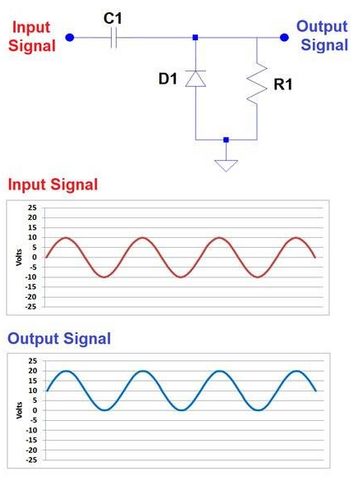
Diodes in clamping circuits
A clamping circuit is used to set the level of either the positive or negative peak of a signal. The input signal is simply added or removed from the dc component. Clampers are also known as IC restorers and ac signal level shifters.
Diodes in reverse current protection
When the voltage at the system's output is greater than the voltage at the input, current flows from the output to the input through the circuit. Reverse current is the name for this type of current. It raises the circuit's power dissipation. Internal electronics, power supply circuits, cables, and connections may be harmed as a result. A diode in series with the supply is the simplest safeguard against the reverse current.

Further to this information, we have more blogs on Diode so if you wish to read them then you may visit our website.